LED sapphire substrate and chip back thinning process
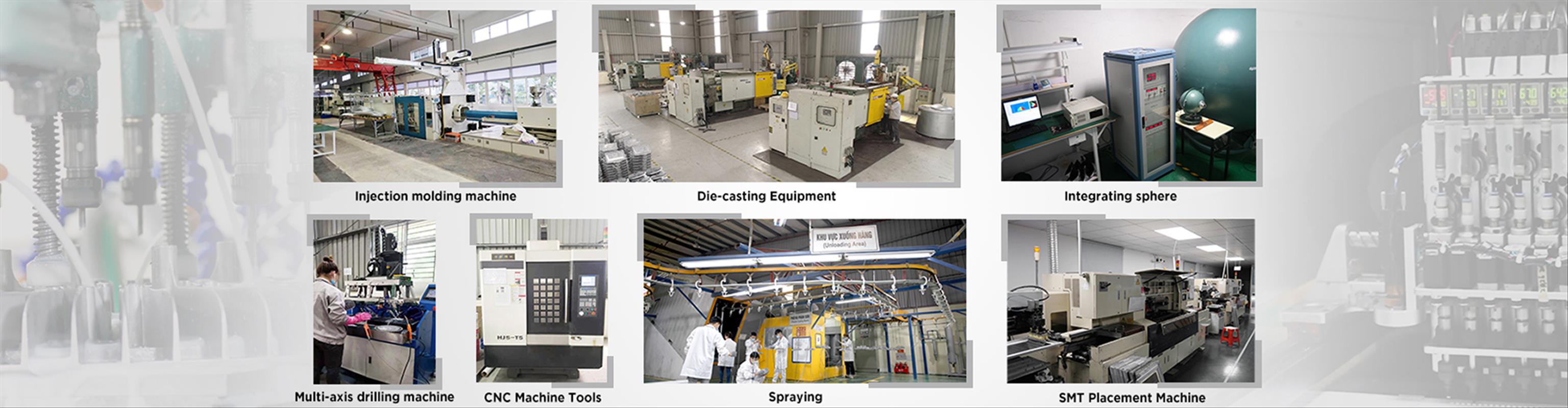
The company is located in:
Currently in the LED process, sapphire substrates from the challenges of Si and GaN substrates, but taking into account the cost and yield, sapphire in the past two years still have an advantage, it is foreseen the next sapphire substrate is the direction of development of large-size and pattern (PSS). As sapphire hardness is second only to diamond, thinning and surface smoothing of it is very difficult. In the gradual exploration, the industry has formed a set of roughly the same sapphire substrate thinning and planarization process.
First, LED sapphire substrate processing technology
First of all, for a sapphire substrate, it has undergone several processes from cutting, roughing, fine grinding, and polishing before it becomes a good substrate. Take 2-inch sapphire as an example:
1. Cutting: Cutting is cut from the sapphire crystal rod through a wire cutting machine to a thickness of about 500um in the film. In this process, diamond wire saw is the most important supplies, mainly from Japan, South Korea and Taiwan.
Rough cast: Sapphire surface after cutting very rough, the need for rough throw to repair the deeper scratches, improve the overall flatness. This step is mainly 50 ~ 80um of B4C plus Coolant grinding, grinding the surface roughness Ra about 1um or so.
3. Fine polishing: The next is more sophisticated processing, because the final product directly related to the yield and quality. The current standard 2-inch sapphire substrate thickness of 430um, so the total removal of fine throwing about 30um or so. Taking into account the removal rate and the final surface roughness Ra, this step is mainly to polycrystalline diamond liquid with resin tin plate Lapping processing.
Most sapphire substrate manufacturers in pursuit of stability, and more use of Japan's grinding machine and the original polycrystalline diamond solution. However, with the increase of cost pressure and the improvement of the domestic consumable standard, the domestic consumable products can replace the original products at present, and the cost is reduced significantly.
Speaking of polycrystalline diamond fluid may wish to say a few words, for the polycrystalline diamond powder part of the powder, the general requirements of the particle size to be concentrated, the shape should be regular, so that it can provide lasting cutting force and surface scratches more evenly. The domestic manufacturers can produce polycrystalline diamond powder Beijing Guorui and Sichuan long, Guorui or at the same time can produce their own diamond fluid, so the quality and cost has a greater advantage. Diamond innovation recently introduced by the United States, "polycrystalline diamonds," is actually an improvement on ordinary single crystal diamonds. Although the stronger structure provides higher cutting forces, it is also more likely to cause deeper scratches .
4. Polishing: While scratches caused by polycrystalline diamonds are significantly smaller than single-crystal diamonds, they still leave significant scratches on the sapphire surface and therefore undergo a CMP polish to remove any scratches and leave a perfect surface . The CMP process was originally a process for flattening a silicon substrate, which is now also true for sapphire substrates. After CMP polishing process of sapphire substrate after layers of testing to meet the standards of qualified products can be extended to the epitaxial plant epitaxy.
Second, the back of the chip thinning process
After the epitaxial, the sapphire substrate becomes an epitaxial wafer. After the epitaxial wafer is subjected to a series of complicated semiconductor processes such as etching, evaporation, electrode fabrication, and protective layer fabrication, the wafer needs to be cut into a granular chip. According to the size of the chip, A 2-inch wafer can be sliced into tens to thousands of CHIPs. As mentioned earlier, the thickness of the epitaxial wafers is around 430 um. Due to the hardness and brittleness of the sapphire, the ordinary cutting process is difficult to process. The current common technology is to reduce the epitaxial wafers from 430um to 100um, and then use laser cutting.
1.Ginding process:
The epitaxial wafer Lapping method although the processing quality is better, but the removal rate is too low, the maximum can only reach 3um / min or so, if the full use of Lapping, then this processing takes about 2h, the time cost is too high . The current solution is to add Grinding process before Lapping, through the diamond grinding machine and thinning machine to achieve the purpose of rapid thinning.
2.Lapping process
After thinning and then use about 6um polycrystalline diamond liquid with resin copper plate, both to achieve a higher removal rate, but also to repair the Grinding process leaving a deeper scratch. In general, splitting occurs during the cutting process because the deeper scratches in the Grinding process are not removed, so the requirements for the diamond fluid are relatively high at this time.
In addition to the chip, some chip manufacturers in order to increase the brightness of the chip, after the Lapping process will be plated on the back of the epitaxial wafer copper, the Lapping surface at this time put forward higher requirements. Although some scratches will not cause lobes, but will affect the effect of back plating. At this point you can use 3um polycrystalline diamond solution or less fine for Lapping process, in order to achieve better surface quality.
Related News
- Why use plant growth lights
- After-sales service for ufo high bay light
- Advantages and disadvantages of ultraviolet sterilization
- Another materials have New breakthrough-Graphene is the protagonist
- Why Choose AC DOB LED Light
- will be implemented from April 1
- LED flood light is broken, what should I do?
- UFO high bay lights
- How far and how large a high-power LED floodlight can illuminate
- LED flood light is broken, what should I do?
- Our Factory(Newlamp Lighting)Testing Standards for order UFO high bay lights.
- Module LED Tunnel Flood Light
- Shenzhen Newlamp New Product Launch Linear high bay .similar like Linear light hence the name Features
- The LED Tunnel light used outdoors is very similar to the LED floodlight
- OLED application
- Meet LED lighting needs in multiple markets with a single solution
- Led sensor light is a new type of intelligent lighting products.
- How to Learn about outdoor lighting design,starting with Floodlighting
- 360W LED Linear High Bay Light (Driverless)
- How to working the Microwave Motion Sensor LED UFO High Bay Lights
 Jackson
 sales01@newlamp-lighting.com