Small out of the high light flux density under the trend of LED package substrate
The company is located in:
Small smooth surface more easily match the secondary optics, get a higher center of light, resulting in a small package high power density LED struck. High power density on the package substrate / packaging process / chip / application side of the thermal conductivity of heat put forward high requirements, small smooth LED roughly two categories: SMD and COB surface light source.
In this need to explain, COB is short for chips on board, high power density SMD light sources are actually COB package. (Small History: Today's COB nicknamed the surface light source when it was born, but in a science exchange organized by Guangzhou Bureau of Science and Technology, the speaker specially mentioned that the surface light source is different from the prevailing packaging technology at that time, using the COB Package. Perhaps the COB features obvious and easy to catch, thus popular).
On the small glossy surface of the high light density trend of the package substrate
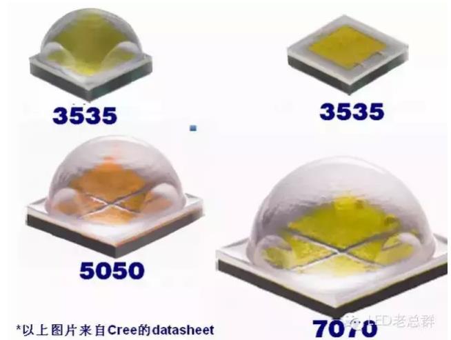
High optical density SMD substrate may be the popular size 3535/5050/7070/9090

Small out of the high light flux density under the trend of LED package substrate
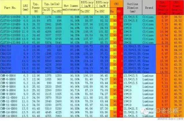
CREE high light density SMD substrate power density
From the table, SMD substrate unit cm 2 power density reaches more than 24W / cm2
Small out of the high light flux density under the trend of LED package substrate
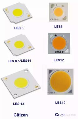
Small smooth high light density COB
COB substrate power density reaches 6W / cm2 above, Cree's 2590 is to reach 14.5W / cm2;
From the tables and reports, a small bright high-pass LES manufacturers generally consistent, 6mm / 8.5mm-9mm / 11mm-12mm / 13mm-14mm / 19mm. Out of the smooth power density between 28-40W / cm2, than ordinary COB power density more than 1 times;
Boldly predict the next 10W below the level of COB surface light source market will be attacked SMD; COB surface light source power density will be as fast as SMD-like promotion, after all, single high-power is its advantage.
High power density package substrate should be met
1 high thermal conductivity
2 higher than the light efficiency
3 chip and substrate thermal expansion coefficient similar to avoid thermal stress on the chip damage
4 anti-oxidation anti-sulfur
5 best thermoelectric separation, mainly for SMD. Thermoelectric separation will greatly facilitate the application side
6 high insulation, mainly for COB surface light source, follow the trend of high voltage and low current non-isolated drive
Small out of the high light flux density under the trend of LED package substrate
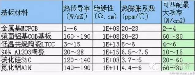
Various types of package substrate data
Compared with high power density SMD, metal-based / SiC / AlN can meet the requirements of heat flux density, but the metal-based and SiC is a conductor and is not suitable for positive and negative pad needs via. Conduction type SMD package substrate, AlN Excellent thermal conductivity and insulation performance is the most suitable high power density package substrate;
Compared with the high power density COB, mirror aluminum / AL2O3 / SiC / AlN can meet the heat flux density requirements. SiC / AlN due to the light efficiency and high cost, the mirror aluminum and Al2O3 ceramic is best suited for small glossy high light through COB package substrate;
Mirror aluminum and Al2O3 ceramic COB package is the two major mainstream. It should be noted that although the thermal conductivity of specular aluminum is much higher than that of ceramics, the more than twenty of its thermal expansion coefficients must account for its thermal stress on the chip substrate at high power densities.
There are also two kinds of Al2O3 ceramic substrates, one is a thick-film sintered silver ceramic substrate, and the other is a late-blooming thin-film DPC (ceramic direct-coated) ceramic substrate.
Small out of the high light flux density under the trend of LED package substrate
DPC is COB substrate
Small out of the high light flux density under the trend of LED package substrate
Sintering silver dress COB substrate
Sintered silver ceramic substrate and DPC ceramic substrate is still quite different, the biggest difference is that DPC substrate is free of silver, will not be oxidized and cured, the lumen maintenance is far better than the sintered silver substrate; package wire pull better than sintered silver substrate; Due to the good affinity of solder for silver, the silver soldering iron soldering iron slightly longer residence time is likely silver solder adsorption off the pad, and DPC pad solderability is far better, the disadvantage of DPC substrate is the initial light Effective as sintering silver substrate, the cost is slightly higher.
DPC through the adhesion, the process of different results vary widely, the process properly, adhesion will be very strong.
Small out of the high light flux density under the trend of LED package substrate
As shown in the tensile test, you can see the ceramics are pulled up
Small out of the high light flux density under the trend of LED package substrate
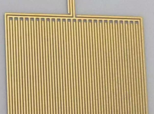
DPC fine line spacing 75um
Small out of the high light flux density under the trend of LED package substrate
DPC flip COB substrate
The future, the COB flip-chip package or vertical structure of the chip package COB will be more suitable for high-pass small COB light source!
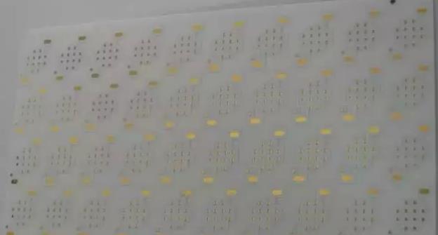
DPC wonderful application:
Small out of the high light flux density under the trend of LED package substrate
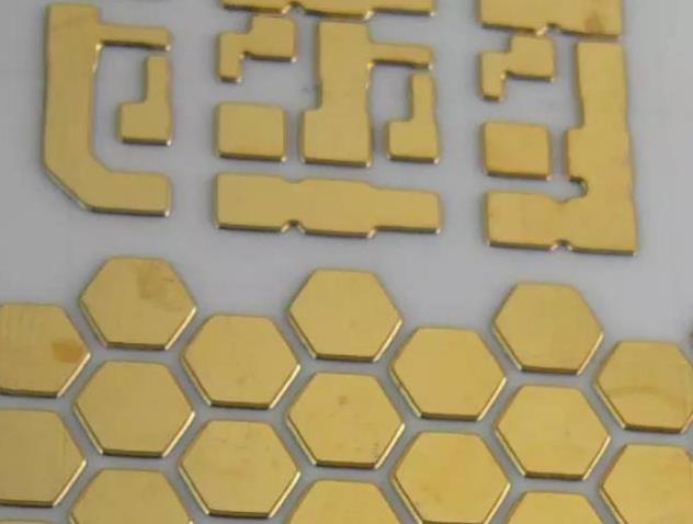
Thick copper high power package substrate
Related News
- LED High Bay Light Brief Introduction
- Vietnam LED lighting market has become the emerging focus?
- LED Outdoor Lighting
- Hong Kong-Zhuhai-Macao Bridge
- LED lamp bead welding process dead lamp reason
- Why there is no street light on the highway? - Dec 29, 2017 -
- LED packaging process, how to do a good job of anti-sulfur measures
- High-power LED lamp beads characteristics and technical parameters
- RGB LED three white LED forming principle
- Improve the light extraction efficiency of thermal resistance power LED pack
- LED packaging Collection: I do not know the LED packaging process knowledge
- LED driver power potting use
- LED flip chip technology and process analysis
- Experimental Study on Improving the Temperature Resistance of LED Light Source
- LED Floodlight structure
- Advantages of Driverless Floodlights
- LED flood light installation instructions
- Advantages Of LED Floodlight
- LED flood light applications
- LED six technology to lead the future


 Jackson
 sales01@newlamp-lighting.com


